| |
|
| |
| |
| |
| |
| |
Research
We conduct research on analog, digital, mixed-signal, and RF Integrated Circuits (IC) design for a variety of applications, including high-speed wireline and wireless communications, data converters, low-power medical devices and instruments, automotive radar, and devices and circuits for radiation, extreme temperature and other harsh environments.
We design high-performance circuits by taking advantage of the speed and digital processing capabilities available in deep submicron and nanometer CMOS technologies to make the circuits low power, easily scalable across technologies, and tolerant to process, voltage, and temperature (PVT) variations. In high-speed communications links design where the data rate is being pushed to tens of Gigabits/s, we explore RF, and millimeter wave (mmwave) design techniques together with digital intensive approach to achieve high-performance as well as good power efficiency and tolerance to PVT variations. We also explore the digital processing capability available in CMOS technologies to design high-performance and low-power analog-to-digital and digital-to-analog converters. In addition, we are designing millimeter-wave circuits (at frequencies of 60 GHz or higher) for anti-collision auto-radar applications as well as medical and defense applications.
In collaboration with CERN (European Particle Physics Laboratory), Fermi National Accelerator Lab, and Brookhaven National Lab, we explore techniques on the system, circuit, and device level to enhance the reliability of circuits operating in radiation or extreme temperature environment. Our approach focuses on innovative circuit-level design and implementation using commercially available mainstream CMOS technologies rather than using expensive specialized technologies. In addition to high-energy physics experiments, these circuits design and implementation techniques can also be applied to commercial applications where tolerance to single-event-effects or software error is becoming more critical with the technologies scaling down to nanometer regime.
Below are some of our on-going research projects.
|
- MM(millimeter)wave circuits IC design.
- Low-Power tens of Gb/s transmitter and receiver ICs.
- High-speed data links for radiation and extreme temperature environments.
- High-speed ADC/DACs.
- Ultra-low-noise amplifier for biomedical applications.
|
|
| |
| |
| |
| |
Design Gallery
|
| |
| |
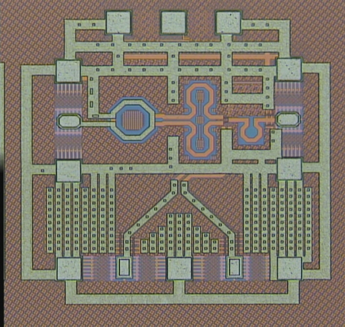
 85-110 GHz CMOS Tunable Nonreciprocal Transmission Line Based Isolator |
The first CMOS nonreciprocal transmission
line (TL) for wideband tunable full-duplex transceiver front
ends, having over 45 dB isolation in a bandwidth of 1.5 GHz
and tuning range of 85-110 GHz, is demonstrated. Offering
tunable nonreciprocal propagation, this structure is based
on a parametric time-varying TL modulated by a 10 GHz
signal through distributed capacitive mixing. Two capacitive
mixers together with a biasing network form a resonant type
of wideband matching. Implemented in a chip area of 0.245
mm2 in 65 nm CMOS, this nonreciprocal TL achieves over
45 dB isolation throughout its entire bandwidth, a maximum
6.5 dB insertion loss (IL) and over 10 dB return loss.
C. Yang, P. Gui, et al, IEEE RFIC 2017.
|
|
| |
| |
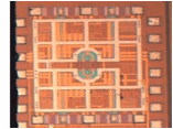
 68-78GHz Transmitter (Mixer+PA) |
A direct-conversion transmitter consisting of a three-stage PA and a double balanced passive up-mixer is designed and implemented in 65nm CMOS process. It achieves a Psat of 14.6 dBm, a peak efficiency of 13.9% and a conversion gain of 15.6 dB.
T. Xi, P. Gui, et al, IEEE TCASII, Vol. 64, Iss. 3, 2017.
|
|
| |
| |
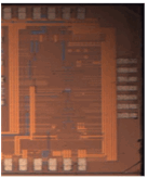
 68-78GHz PA |
Employing our proposed gate capacitance linearization technique and the serial combining method, this three-stage PA, implemented using 65nm CMOS process, achieves a saturated power (Psat) of 17.3 dBm, a peak PAE of 18.9% and a maximum gain of 21.4 dB over 58-78GHz frequency range.
T. Xi, P. Gui, et al, IEEE TCASII, Vol. 64, Iss. 3, 2017.
|
|
| |
| |
 60GHz Mixer |
A CMOS mmW passive mixer topology based on a novel LO shaping technique using non-linear transmission line (NLTL) is proposed. It boosts the LO swing and re-shapes the LO pulses to have higher amplitude, narrower pulses, and sharper edges, resulting in higher gain, better linearity, and lower NF for the mixer. Mixers operating at 60GHz are designed using 65nm CMOS process. Simulation results show the mixer with the proposed technique obtains an NF of 5.9dB, input referred P1dB (IP1dB) of 0.9dBm, and voltage conversion gain of 1.2dB with 0dBm LO signal and 0 DC power. Silicon measurement results show that LO shaping technique improves the conversion gain by 2.5 dB and the IP1dB by 3 dB.
T. Xi, P. Gui, et al, IEEE Microwave and Wireless Components Letters(MWCL),Vol. 26, Iss. 6, 2016.
|
|
| |
| |
 25Gb/s 0.6V low-power CDR |
A novel low-power low-jitter 25 Gb/s serial-link CDR that can work at an ultra low supply voltage of 0.6 V is designed and implemented in a 65 nm CMOS process. A two-tank transformer-feedback technique is proposed in the 25 GHz LC-tank VCO to improve the phase noise performance at low supply voltage. Forward-body biasing (FBB) technique is proposed in the low-voltage signal path to reduce the threshold voltage of the transistors, increasing the signal amplitude and achieving low BER. The measurement results show that the CDR can work under 0.6 V with 0.23ps/4.62ps (rms/pk-pk) of recovered clock jitter. The measured power consumption of the CDR is 39.6 mW (1.58 mW/Gb/s).
S. Guo, P. Gui, et al, IEEE RFIC 2015.
|
|
| |
| |
 77GHz PA |
A new design technique is employed in this class-AB mmwave power amplifier to improve its gate capacitance linearity and power efficiency. Implemented in 65 nm CMOS process, the presented PA consists of two differential stages, uses baluns, transformers and inductors to realize the input, output, and inter-stage power matching, and achieves a peak PAE of 24.2%, a 6 dB back-off PAE of 10.5% from 3 dB gain compression, a maximum gain of 17 dB, and a 3-dB bandwidth from 68 to 78 GHz
T. Xi, P. Gui, et al, IMS 2015.
|
|
| |
| |
 60GHz LNAs |
A transformer feedback gm-boosting technique is proposed in a single-ended cascode topology to increase the gain and reduce the noise. Fabricated in a 65 nm CMOS process, the transformer-based (TF-based) LNA exhibits a minimum noise figure (NF) of 3.6 dB at 53.5 GHz and a highest power gain of 28.2 dB at 54 GHz in measurement.The transmission-line-based (TL-based) LNA exhibits a minimum noise figure of 3.8 dB at 53.9 GHz and a highest power gain of 25.4 dB at 54.2 GHz in measurement. Both the LNAs consume 18 mA from a power supply of 1.1 V.
S. Guo, P. Gui, et al, IEEE ASSCC 2014, IEEE Transactions on Microwave Theory and Techniques (TMTT), Vol 64, Iss. 7, 2016.
|
|
| |
| |
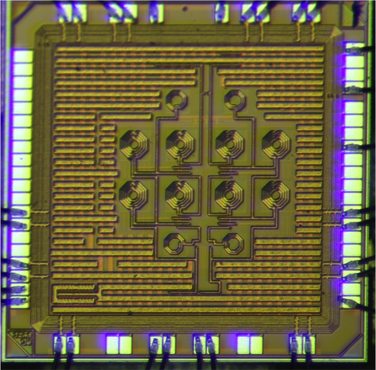
 54GHz QVCO and 76/90GHz VCO |
A transformer coupling with extra phase shift is proposed in QVCO to decouple the tradeoff between phase noise (PN) and phase error and improve the PN performance. This technique is demonstrated in a mmWave QVCO with a measured PN of - 119.2dBc/Hz at 10MHz offset of a 56.2GHz carrier and a tuning range of 9.1%. An inductive divider feedback technique is proposed in mmwaveVCO design to improve the transconductance linearity, resulting in larger signal swing and lower PN . The effectiveness of this approach is demonstrated in a 76GHz VCO and a 90GHz VCO, both fabricated in a 65nm CMOS process, with an FOMT of 173.6dBc/Hz and 173.1dBc/Hz respectively.
T. Xi, P. Gui, et. al, IEEE RFIC 2014, IEEE Transactions on Microwave Theory and Techniques (TMTT), Vol 64, Iss. 7, 2016.
|
|
| |
| |
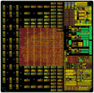
 1-16Gb/s Any-date-Rate CDR |
An all-digital phase interpolator (PI)-Based clock and data recovery (CDR) is designed to accommodate any data rate continuously from 1 to 16 Gb/s with quadrature sampling clocks from 4 to 8 GHz. The CDR core occupies 0.088 mm2 in 65 nm CMOS technology and consumes 73.1 mA at 16 Gb/s from a 1.2 V supply. Measurement results show that this CDR can function at any date rate from 1-16Gbps and is able to exceed the SONET OC-192 jitter tolerance mask at least by 0.2 UI at high frequencies (4-100 MHz).
G. Wu, P. Gui, et al, IEEE Transactions on Very Large-Scale Integration (VLSI) Systems, Vol. 24, Iss. 7, 2016
|
|
| |
| |
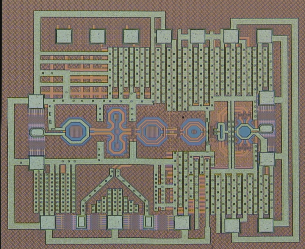
 10Gb/s Laser Driver |
The GigaBit Laser Driver (GBLD) is a key on-detector component of the GigaBit Transceiver (GBT) system for CERN's SLHC experiments. Employing the distributed-amplifier (DA) architecture, this radiation-tolerant GBLD driver chip able to push the data rate to 10 Gb/s implemented using a 130nm CMOS process, driving VCSELs with modulation currents up to 12 mA, with a power consumption of 85mW.
T. Zhang, P. Gui, et al, IEEE Transactions on VLSI Systems, Vol. 24, Iss. 7, 2016
|
|
| |
| |
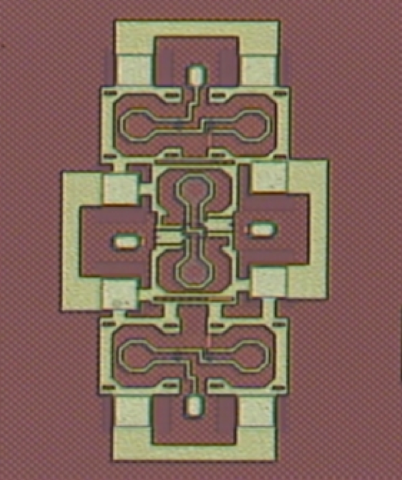
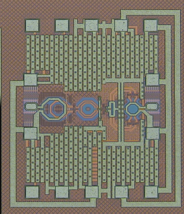
 5Gb/s Serializer/Deserializer |
This design presents a wide-range (25 ns) and high-resolution (48.8 ps) clock phase shifter developed and fabricated using a 130nm CMOS technology. Test results show that the standard deviations of the DNL and INL are 4.7 ps and 4.3 ps respectively.
G. Wu, P. Gui, et. al, IET Electronics Letters, Volume 49, Issue 10, pp642-644, Oct.2013.
P. Moreira, et al, Journal of Instruments, 2010.
|
|
| |
| |
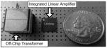
 5Gb/s Transimpedance Amplifier (TIA) |
A 5 Gb/s radiation-tolerant fully-differential optical receiver is designed and implemented in a commercial 130nm CMOS process. Measurement results show that the GBTIA displays a sensitivity better than -19 dBm for a BER of 10-12. The differential output across an external 100 W load remains constant at 400 mVpp even for signals near the sensitivity limit. The chip achieves an overall transimpedance gain of 20 kW at the worst case. The total power consumption of the chip is less than 120 mW and the chip die size is 0.75 mm x 1.25 mm. Irradiation testing of the chip shows basically no performance degradation after a total ionization dose of 200 Mrad.
M. Menouni, T. Xi, P. Gui, and P. Moreira, IEEE Transactions on Nuclear Science, Vol 60, Iss 4, pp.3104-3109, Aug. 2013.
|
|
| |
| |
 5Gb/s Laser Driver |
A laser driver for data transmission at 5 Gb/s has been developed as a part of the Giga Bit Transceiver (GBT) project. The GBLD ASIC can drive both VCSELs and some types of edge emitting lasers.
G. Mazza, P. Gui, P. Moreira, et. al, IEEE Transactions on Nuclear Science, Vol. 59 , Iss. 6, pp. 3229 - 3234 , Dec. 2012.
|
|
| |
| |
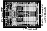
 180Vpp Ultrasound Transmitter Driver With Current Feedback |
This design presents a novel integrated high-voltage linear power amplifier for medical ultrasonic transmitters. The amplifier employs current-feedback technique with two cascading push-pull class-AB buffers to overcome the gain-bandwidth product limitation of a conventional voltage-feedback amplifier, capable of generating high output signal swing with a wide closed-loop bandwidth.
Z. Gao, P. Gui, et al, IEEE TCAS-II. Vol. 61, Iss. 6, pp. 373-377, June 2014.
Z. Gao, and P. Gui, IEEE TUFFC, vol. 59, no. 7, July 2012.
|
|
| |
| |
  180V Linear Amplifier for Ultrasound Transmitter |
This design presents a monolithically integrated fully differential linear high-voltage (HV) amplifier as the driver of an ultrasonic transducer, capable of transmitting HV arbitrary signals with very low harmonic distortion, suitable for Tissue Harmonic Imaging and other ultrasonic modes for enhanced imaging quality. The amplifier is designed and implemented using a 0.7 um CMOS Silicon-On-Insulator (SOI) process with 120V devices.
K. Sun, P. Gui, et. al, IEEE TCAS-II, in press.
|
|
|
|
| |
| |
| |
| |
Sponsors
We thank our sponsors for supporting our research.
|
|
|
|
|
|
|